X006
Datasheet
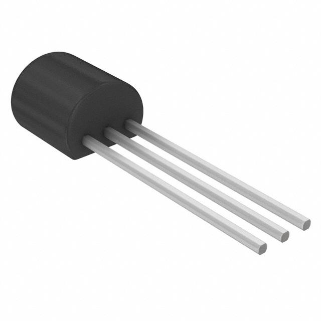
0.8 A 600 V logic level gate thyristor SCR in TO-92 package
A
Features
•
On-state RMS current, IT(RMS) 0.8 A
K
•
•
•
Repetitive peak off-state voltage 600 V
Triggering gate current 200 μA
ECOPACK2 compliant
G
Applications
K
TO-92 (preform)
G
A
TO-92 (straight)
K
G
A
•
•
•
•
•
•
Limited gate current topologies
Ground fault circuit interrupters
Overvoltage crowbar protection in power supplies
Protection in electronic ballasts
Capacitive discharge ignitions
Ignitors (lighting, oven...)
Product status link
Description
X006
Product summary
IT(RMS)
0.8 A
VDRM/VRRM
600 V
IGT
200 µA
Tjmax.
125 °C
Available in through hole package, the X006 SCR can be used as on/off function in
applications where topology does not offer high current for gate triggering.
This device is optimized in forward voltage drop and inrush current capabilities for
reduced power losses and high reliability in harsh environments.
Thanks to its highly sensitive triggering current the X006 is suitable for the
applications such as breaker, ground fault interrupter, overvoltage crowbar protection
of power supplies or capacitive ignition circuits.
DS1704 - Rev 6 - January 2022
For further information contact your local STMicroelectronics sales office.
www.st.com
�X006
Characteristics
1
Characteristics
Table 1. Absolute maximum ratings (limiting values, Tj = 25 °C unless otherwise specified)
Symbol
IT(RMS)
IT(AV)
ITSM
I2t
dl/dt
IGM
PG(AV)
Tstg
Tj
Parameters
Value
Unit
On-state RMS current (180° conduction angle)
TO-92
TL = 83 °C
0.8
A
Average on-state current (180° conduction angle)
TO-92
TL = 83 °C
0.5
A
Non repetitive surge peak on-state current,
tp = 8.3 ms
Tj initial = 25 °C
tp = 10 ms
I2t value for fusing
tp = 10 ms
Tj = 25 °C
0.4
A2s
F = 60 Hz
Tj = 125 °C
50
A/µs
tp = 20 µs
Tj = 125 °C
1
A
Tj = 125 °C
0.1
W
Storage junction temperature range
-40 to +150
°C
Operating junction temperature range
-40 to +125
°C
Critical rate of rise of on-state current
IG = 2 x IGT , tr ≤ 100 ns
Peak gate current
Average gate power dissipation
10
Tj = 25 °C
A
9
Table 2. Electrical characteristics (Tj = 25 °C, unless otherwise specified)
Symbol
IGT
Parameters
Value
VD = 12 V, RL = 140 Ω
VGT
Unit
Min.
15
Max.
200
Max.
0.8
V
V
µA
VGD
VD = VDRM, RL = 3.3 kΩ, RGK = 1 kΩ, Tj = 125 °C
Min.
0.2
VRG
IRG = 10 µA
Min.
5
IH
IT = 50 mA, RGK = 1 kΩ
Max.
5
mA
IL
IG = 1 mA, RGK = 1 kΩ
Max.
6
mA
VD = 67 % VDRM, RGK = 1 kΩ, Tj = 125 °C
Min.
25
V/µs
Value
Unit
dV/dt
Table 3. Static electrical characteristics
Symbol
Test conditions
VTM
ITM = 1 A, tp = 380 µs
25 °C
Max.
1.35
V
VTO
Threshold on-state voltage
125 °C
Max.
0.85
V
Rd
Dynamic resistance
125 °C
Max.
245
mΩ
IDRM
VDRM = VRRM, RGK = 1 kΩ
25 °C
IRRM
VDRM = VRRM, RGK = 1 kΩ
125 °C
Max.
1
100
µA
Table 4. Thermal resistance
Symbol
DS1704 - Rev 6
Max.
value
Parameters
Rth(j-l)
Junction to leads (DC)
TO-92
70
Rth(j-a)
Junction to ambient (DC)
TO-92
150
Unit
°C/W
page 2/9
�X006
Characteristics (curves)
1.1
Characteristics (curves)
Figure 1. Maximum average power dissipation versus
average on-state current
Figure 2. Average and DC on-state current versus lead
temperature (TO-92)
P(W)
IT(AV) (A)
0.6
1.0
α = 180°
TO-92
0.9
0.5
D.C.
0.8
0.7
0.4
0.6
α = 180°
0.5
0.3
0.4
0.2
0.3
360°
0.2
0.1
0.1
α
IT(AV) (A)
0.0
0.1
0.2
Tl (°C)
0.0
0.0
0.3
0.4
0.5
0
0.6
25
50
75
100
125
Figure 3. Average and DC on-state current versus ambient Figure 4. Relative variation of thermal impedance junction
temperature (epoxy printed circuit board FR4, copper
to ambient versus pulse duration (PCB FR4, copper
thickness = 35 µm, SCU = 0.5 cm2)(TO-92)
thickness = 35 µm, SCU = 0.5 cm2)(TO-92)
Zth(j-a) /Rth(j-a)
IT(AV) (A)
1.0
1.00
TO-92
SCU = 0.5 cm2
TO-92
SCU = 0.5 cm2
0.9
D.C.
0.8
0.7
0.6
α = 180°
0.5
0.10
0.4
0.3
0.2
0.1
Tamb (°C)
t p (s)
0.0
0
25
50
75
100
125
Figure 5. Relative variation of gate trigger, holding and
latching current versus junction temperature (typical
values)
IGT,IH,IL [ Tj ] / IGT,IH,IL [T j =25°C]
0.01
1.E-03
1.E-01
1.E+00
1.E+01
1.E+02
1.E+03
Figure 6. Relative variation of holding current versus
gate-cathode resistance (typical values)
3.5
1.6
1.E-02
IH[R GK ] / IH[ RGK =1kΩ]
3.0
1.4
2.5
1.2
2.0
1.0
IH & IL
0.8
1.5
0.6
IGT
1.0
0.4
0.5
0.2
Tj (°C)
0.0
-40 -30 -20 -10
DS1704 - Rev 6
0
10
20
30
40
50
RGK (kΩ)
0.0
60
70
80
90 100 110 120 130
1.E-02
1.E-01
1.E+00
1.E+01
1.E+02
page 3/9
�X006
Characteristics (curves)
Figure 7. Relative variation of static dV/dt immunity
versus gate-cathode resistance (typical values)
Figure 8. Relative variation of static dV/dt immunity
versus gate-cathode capacitance (typical values)
dV/dt[R GK ] / dV/dt[ RGK =1kΩ]
100
100.0
dV/dt[C GK ] / dV/dt[R GK =1kΩ]
VD = 0.67 x VDRM
RGK = 1kΩ
VD = 0.67 x VDRM
10.0
10
1.0
RGK (kΩ)
CGK (nF)
0.1
1.0E-01
1.0E+00
1
1.0E+01
1
Figure 10. Non-repetitive surge peak on-state current for
sinusoidal pulse (tp< 10 ms)
Figure 9. Surge peak on-state current versus number of
cycles
10
10
ITSM(A)
ITSM(A)
1.E+02
Tj initial = 25 °C
9
8
ITSM
tp = 10 ms
7
One cycle
1.E+01
Non repetitive
Tj initial = 25 °C
6
5
4
Repetitive
TC = 83 °C
1.E+00
3
2
1
t p (ms)
Number of cycles
0
1
10
1.E-01
100
1000
0.01
0.10
1.00
10.00
Figure 11. On-state characteristics (maximum values)
ITM(A)
10.00
Tj max.:
Vt0 = 0.85 V
Rd = 245 mΩ
1.00
Tj = 125 °C
Tj = 25 °C
0.10
VTM(V)
0.01
0.0
DS1704 - Rev 6
0.2
0.4
0.6
0.8
1.0
1.2
1.4
1.6
1.8
2.0
2.2
2.4
2.6
2.8
3.0
page 4/9
�X006
Package information
2
Package information
In order to meet environmental requirements, ST offers these devices in different grades of ECOPACK packages,
depending on their level of environmental compliance. ECOPACK specifications, grade definitions and product
status are available at: www.st.com. ECOPACK is an ST trademark.
2.1
TO-92 with straight leads (plastic) package information
•
•
Lead free plating + halogen-free molding resin
Epoxy meets UL94, V0
Figure 12. TO-92 with straight leads (plastic) package outline
c
A
a
B
C
b
D
F
E
Table 5. TO-92 with straight leads (plastic) package mechanical data
Dimensions
Inches(1)
Millimeters
Ref.
Min.
A
Typ.
Max.
Min.
1.35
B
Typ.
0.048
4.70
C
Max.
0.190
2.54
0.100
D
4.40
0.172
E
12.70
0.554
F
3.70
0.152
a
0.50
0.022
b
1.27
c
0.050
0.48
0.019
1. Inches dimensions given for information
DS1704 - Rev 6
page 5/9
�X006
TO-92 with leads preform (plastic) package information
2.2
TO-92 with leads preform (plastic) package information
•
•
Lead free plating + halogen-free molding resin
Epoxy meets UL94, V0
Figure 13. TO-92 with leads preform (plastic) package outline
Table 6. TO-92 with leads preform (plastic) package mechanical data
Dimensions
Inches(1)
Millimeters
Ref.
Min.
Typ.
Max.
Min.
Typ.
Max.
G
1.30
1.70
2.00
0.051
0.067
0.079
H
7.69
9.69
0.303
0.381
d
2.40
2.90
0.094
0.114
θ
30°
50°
30°
40°
40°
50°
1. Inches dimensions given for information
DS1704 - Rev 6
page 6/9
�X006
Ordering information
3
Ordering information
Figure 14. Ordering information scheme
X
006
02
M
A
1AA2
Sensitive SCR series
Current
006 = 0.8 A
Sensitivity
02 = 200 µA
Voltage
M = 600 V
Package
A = TO-92
Packing mode
1AA2 = Bulk (TO-92 with straight leads)
2AL2 = Ammopack (TO-92 with leads preform)
5AL2 = Tape and reel (TO-92 with leads preform)
Table 7. Ordering information
Order code
Marking
X00602MA 1AA2
X00602MA 2AL2
X00602MA 5AL2
DS1704 - Rev 6
X0602 MA
Package
Weight
Base qty.
Delivery mode
TO-92 straight leads
0.2 g
2500
Bulk
0.2 g
2000
Ammopack
0.2 g
2000
Tape and reel
TO-92 leads preform
page 7/9
�X006
Revision history
Table 8. Document revision history
DS1704 - Rev 6
Date
Revision
Changes
26-May-2009
3
Last update.
03-May-2012
4
SOT-223 package added.
03-Sep-2021
5
Reformatted to current standards. Device X00605 removed. Updated
dimensions in Table 5.
18-Jan-2022
6
Removed SOT-223 package information. Added Section 2.2 TO-92 with
leads preform (plastic) package information.
page 8/9
�X006
IMPORTANT NOTICE – PLEASE READ CAREFULLY
STMicroelectronics NV and its subsidiaries (“ST”) reserve the right to make changes, corrections, enhancements, modifications, and improvements to ST
products and/or to this document at any time without notice. Purchasers should obtain the latest relevant information on ST products before placing orders. ST
products are sold pursuant to ST’s terms and conditions of sale in place at the time of order acknowledgement.
Purchasers are solely responsible for the choice, selection, and use of ST products and ST assumes no liability for application assistance or the design of
Purchasers’ products.
No license, express or implied, to any intellectual property right is granted by ST herein.
Resale of ST products with provisions different from the information set forth herein shall void any warranty granted by ST for such product.
ST and the ST logo are trademarks of ST. For additional information about ST trademarks, please refer to www.st.com/trademarks. All other product or service
names are the property of their respective owners.
Information in this document supersedes and replaces information previously supplied in any prior versions of this document.
© 2022 STMicroelectronics – All rights reserved
DS1704 - Rev 6
page 9/9
�
很抱歉,暂时无法提供与“X00602MA 5AL2”相匹配的价格&库存,您可以联系我们找货
免费人工找货